DIY S-603W / RH-1X1128AFZZ replacement for Optonica SM-7100

There are a few designs floating around for replacing this darlington hybrid online, but none of them seem to be very well tested. I created this design by tearing down, measuring and reverse-engineering a fully functional S-603W. The most important change to the design compared to the original hybrid, is the addition of a bias adjustment potentiometer. The resistors are laser-cut in the original hybrids to permanently set bias, and that’s just not practical when manufacturing discrete replacements. You also can’t just copy the original bias resistor value verbatim, as you’re very likely to be using more modern transistors with higher gain than the ones in the hybrid (the original 992/1845 had under 200 hFE – yikes!) The result of copying the values of a hybrid straight off is likely to give you an amplifier with no bias at all, and no way to adjust it.

The transistors used can be pretty much anything. The 992/1845 are a good jellybean choice, but for the following two stages, “any decent >120V hifi driver transistor pair” and “any decent >120V hifi power transistor pair” will work. The ones I used came from a scrapped Onkyo AVR. You might be able to use integrated darlington pairs for the two last stages, at the cost of slightly higher distortion.

Bias
Since the resistor by the diodes ends up being a much higher value than the original design (original in my module was 61 ohm, my potentiometers ended up being set at about 400 ohm), the diodes have less authority over the bias reduction as the heat sinks warm up. Bias is increased by adding more resistance in series with the diodes. This means that the higher the bias is set, the less authority the diodes have to decrease the bias with temperature, and the more likely the module is to thermally run away when it gets hot. For this reason, it’s important to keep bias low. Crossover distortion disappears well below 20 mA bias, so there’s no point setting it higher! Thermal runaway becomes very likely if the bias is set to more than 30 mA when allowed to warm up with no load. 20 mA is about 5 mV across the test points in an Optonica SM-7100.

Actually constructing the module was reasonably simple with these transistors since the pinouts are very easy to work with:

The small copper sheets double as heat sinks for the driver transistors, and serve to couple the base of the right hand side 992 to the other side of the “transistor stack”. The drive transistors turned out not to need any cooling – they run quite cool. The 992/1845 run at about 60 C in normal operation with no cooling, and don’t get much warmer under load.

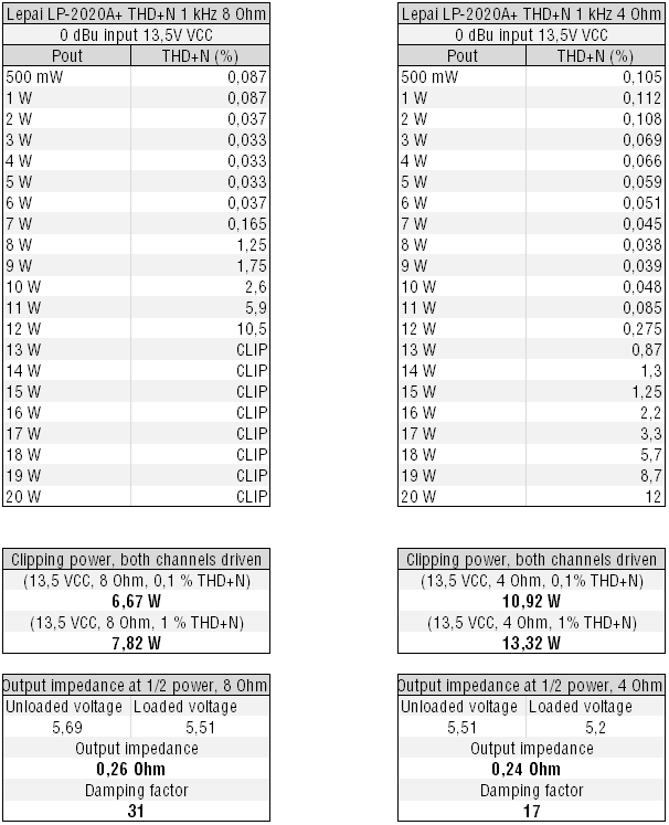
I’ve tested these modules extensively, and they’ve survived continuous rated power, 4-ohm loading and even an output short-circuit. Performance is excellent, and you can find a test report of the finished amplifier here.

Other “fixes”

If you want to cut down on the preamp noise, you can change the power stage feedback resistors R335/R336 (R335 was misprinted as R349 on my PCB, so watch out! It’s the smaller “R349”) from 10K to 8K2 to decrease the amplifier’s gain by a couple of dB, and change the input series resistors R303/R304 from 1K to 10K. These mods combined increase the input impedance to 20k and drop the power amplifier’s gain from 26 dB to 18 dB, which really makes the preamp’s hiss a lot less noticeable, and makes the amp more compatible with modern sources like computers and CD players.

The bass knob is generally quite terrible on this model, adding gain all the way up to 400 Hz. adding a 22 nF film cap across C215 and C214 right next to the bass knob will drop the frequency down a bit, making it sound a bit more pleasant:

Yamaha P-2200 measurements

Yamaha P-2200 uncased

Yamaha P-2200 PA power amplifier

Measurement results for Yamaha P-2200

Measurement results for Yamaha P-2200

PDF version

After many hours of work, I finally got my Yamaha P-2200 into a state worthy of being tested. The left channel is 100 % original, save for new electrolytic capacitors. It should be fairly representative of a completely original unit. The right channel has received major repairs. The high vol = FS noise floor on the right channel is not due to the repairs done to the amplifier, but rather the factory wiring of the amplifier; it’s mostly made up of 50 Hz hum. There’s probably a signal wire going too close to the transformer, somewhere.

All in all, the Yamaha P-2200 is a very well-performing amplifier, especially for its age and the fact that it’s Yamaha’s first ever dive into the world of PA amps. With plenty of passively-cooled power, tank-like build quality, an impressive noise floor and a good damping factor to boot, Yamaha made sure to make their PA power amp début one for the ages!

Just for fun, four audio gear gifs!

These files are huge (about 3 MB each), so give it some time to load!

JVC SEA-M9 in spectrum analyser mode

JVC SEA-M9 in spectrum analyser mode

The JVC SEA-M9 in spectrum analyser mode, filmed during an earthquake.

The JVC SEA-M9 in spectrum analyser mode, filmed during an earthquake.

The dancing meters of the Yamaha P-2200

The dancing meters of the Yamaha P-2200

Freshly refoamed Acoustic Research AR-7 woofer doing its thing.

Freshly re-foamed Acoustic Research AR-7 woofer doing its thing.

Substituting the SFC6120 double transistor in the Tandberg TR-1055

Tandberg TR-1055

Tandberg TR-1055

This nice-looking unit came into the shop with a noisy left channel as well as an intermittent DC offset. After seemingly repairing it by replacing the output transistors, the customer returned it complaining about the same issue arising after a few hours of use. After some further troubleshooting, the problem was found to be a Motorola-branded double transistor in the power amplifier.

The SFX6120 double transistor

The SFC6120 double transistor in the negative feedback circuit

Neither the part nor a datasheet for it was anywhere to be found, so a substitute had to be manufactured. I settled for a matched pair of the common KSC1845 to do the job. Gain matching is important, as an unmatched pair will result in a DC offset on the output of the amplifier.

Installing the transistors is easy, as the pin-out for the SFC6120 is printed on the circuit board.

Transistor 1 installed

Transistor 1 installed

Both replacement transistors installed

Both replacement transistors installed

However, my KSC1845s had roughly twice the gain of the SFC6120 (380 vs. 160), which resulted in a considerable increase of the amplifier’s gain. To counteract this, feedback resistor R712 was decreased from 10 kOhm down to 3,6 kOhm.

R712, the blue resistor, determines the gain of the amplifier module

R712, the blue resistor, determines the gain of the amplifier module

Since the modification altered the gain of the amplifier, I decided to perform it on both channels to ensure proper matching and guard against future SFC6120 failures. It is important to ensure thermal coupling between the two transistors, in order to guard against DC offset when the amplifier warms up. That’s probably why Tandberg decided to use a double transistor in the first place.

Somewhat unexpectedly, the THD+N of the amplifier decreased from 0,08 % at rated output into 4 Ohm, to a mere 0,033 % after the modification. (Measured with my HP 339A at 1 kHz)

After many hours of heavy load testing into 4 Ohm, I think this unit is ready to go back to the customer again – and hopefully not return!

The finished pair of output modules

The finished pair of output modules. Note the thermal goop on the KSC1845s. The two modules have been (partially) recapped at different occasions.

An untouched Tandberg TR-1055 output module

An untouched Tandberg TR-1055 output module (For reference)

Yamaha AX-590 measurements


Yamaha AX-590 integrated amplifier

Yamaha AX-590 integrated amplifier

AX-590_results

For kicks, I thought I’d do a basic THD+N test on my Yamaha AX-590. The results are next to stunning – this is an extremely capable unit. The -88 dBV noise floor (measured with shorted input, CD Direct enabled and the volume at -inf) is simply fantastic for a 100 WPC amplifier, and I had to check that my test load wasn’t broken when measuring the damping factor – almost 1000 at 1 kHz!

What a performer! Given the relatively low (about $600 in 1996) retail price of this unit, I did not expect it to perform anywhere near this well.

Lepai LP-2020A+ mini-review and measurements

Thanks goes out to a friend for donating this amplifier for testing! (You know who you are)

You can hardly enter five forum threads on budget audio without seeing the Lepai LP-2020A+ mentioned. At about 20 U.S. dollars (30 with an AC adapter included), this compact and 20 WPC advertised amplifier looks like a solid deal.

However, despite its popularity, actual information about it seems scarce, aside from the occasional teardown or two. It’s built around a Tripath TA2020-020 class D amplifier chip, which, with its fine specifications and almost 90% efficiency, is what allows for this fantastic power to size ratio.

The specifications printed on the box (that’s apparently used for two models)

However, class D amplifiers require far more attention to detail in the circuit board design and component selection than traditional class AB chip-amps (like the classic LM3886). Did Lepai get it right? Does the LP-2020A+ live up to the specifications quoted on the box, or perhaps even the ones quoted in the TA2020-020 datasheet?

Let’s find out! (The less technically minded may want to skip to the verdict)

The test set-up

The test set-up

The LP-2020A+ was powered by a 5 A industrial switchmode power supply. THD+N measurement was done with an HP 339A, low-passed at 30 kHz. A 4/8 Ohm switchable resistive load was used.

Output impedance/damping factor was calculated by setting a loaded voltage of 5,51 V (8 Ohm) and 5,2 V (4 Ohm) and observing the voltage change when the load was disconnected. A VCC of 13,5 V was used for all tests, 13,4 V was the lowest voltage observed.

The results (updated 9.12.2012):

lepai_results

A-weighted spectrum captured at 5 W into 8 Ohm.

More spectrums (HF noise is included in the unweighted ones):

Sadly, but perhaps not surprisingly, the Lepai did not fulfil the claimed 20 W/ch at <0,05 % THD.

It starts distorting after about 9,6 W into 4 Ohm and 5,6 W into 8 Ohm. It doesn’t show on the THD+N measurements, but the clipping waveform during mild clipping is unorthodox and in my opinion rather intrusive. It causes a popping sound in the tweeters of my test speakers.

It does however far surpass its specification of 80 dB SNR, measuring in at 90,1 dB A-weighted and 87 dB unweighed from 20 Hz to 20 kHz.

Absolute noise measures in at roughly -76 dBV(a). This is 10 dB higher than higher-end amplifiers I’ve measured, and can be audible on many speakers – it is very obvious on mine. If noise above the audible spectrum is included, the numbers falls considerably; if measured unweighted from 10 Hz through 30 kHz on my HP 339A, the noise floor is at roughly -66 dBV. For comparison, that’s nearly two orders of magnitude above the -84 dBV of the Luxman L-120A that resides in my system.

The LP-2020A+ exhibits this behaviour during mild clipping. Picture taken at 0,3 % THD+N.

There is also a constant 200 mV P-P noise at about 160 kHz. Even with the low-pass filters in place, this somehow caused the 339A to go haywire when measuring at very low levels (<250 mW). This noise is probably not an issue in everyday use.

There is a constant noise present at about 160 kHz.

Scope view of a 20 kHz sine wave at 5 W into 8 Ohm. The HF noise can be seen as the abnormal thickness of the trace.

A more noteworthy detail about the LP-2020A+ is that it seems to have a considerable notch in the frequency response above 10 kHz, even with the tone controls disabled. After investigating the issue, I was able to conclude that the notch was not present at the input of the TA2020-020 amplifier chip.

Captured at the output, this curve shows that the frequency response peaks at about +1,6 dB at 30 kHz, and is up by over 1 dB at 20 kHz.

I’m not certain about what causes this anomaly, but I’d wager that it has to do with the way Lepai have designed the output filter. This could very well be an audible problem with this amplifier.

The high-frequency anomaly aside, the LP-2020A+ seems to be flat throughout the frequency spectrum down to about 40 Hz, rolling off by 1 dB at 17 Hz.

Build quality

The LP-2020A+ freed of its case

Build quality wise, you do get what you pay for – the design has a fair few cut corners that deviate from the design guidelines in the TA2020-020 datasheet, in order to reduce component count. The electrolytic capacitors are of varying Chinese brands not renowned for their quality, the potentiometers are pretty nasty and power supply filtering is … minimalistic. All in all, it’s still better than I expected. Soldering quality is decent and the aluminium case is solid.

However, something that struck me about my unit was this:

My LP-2020A+ had very poor heat sink mounting.

Thermal paste was scarce.

Yes, there was an almost millimetre-thick gap between the chip and the heat sink! The over-temperature protection would kick in after a few minutes of heavy 4-Ohm loading. Thanks to the efficiency of the TA2020-020, this would probably not have been noticeable in every-day use. However, one must wonder what it does to the chip lifespan.

Verdict

I entered this with a hunch that the Lepai LP-2020A+ would not deliver its advertised performance. The TA2020-020 chip that it’s built around is rated for 20 W into 4 Ohm at 5 % THD. Despite that, it is still a very decently performing amplifier for the price as long as you stay within its limits. 5 clean Watts per channel into 8 Ohm might not sound like a lot, but for casual near-field listening with small bookshelf speakers it should still be plenty; “normal” background listening level is generally only around 0,1 Watt!

The biggest issue with this unit is the build quality. The casing is good quality extruded aluminium, but the quality control and above all the potentiometers (volume control, bass and treble) are of atrocious quality. The unevenness and scratching of the volume control can be fairly bothersome, especially when close to zero. Since the volume control is connected to adjust the gain of an op-amp rather than simply attenuate the input signal, a bad connection in it can lead to very loud popping and oscillation.

Sound quality wise, there isn’t much to comment on. There is a slight notch in the treble that could colour the sound, but it is a minor issue in this market segment. Other than that LP-2020A+ has a background hiss that’s 10 dB (twice as loud) higher than the considerably more costly amplifier I usually have in my system. Depending on what speakers are used and how sensitive one is to background hiss, this could be an issue, and probably the biggest sound quality concern with the Lepai.

All in all, would I recommend it? The answer is a resounding yes! While it’s hardly “audiophile quality”, you aren’t going to find a better 5-watt-per-channel amplifier for the price – and with proper stereo amplifiers often costing several hundred Dollars, this little Lepai introduces a whole new standard for budget amplification.

Image gallery

Front

Rear

Top

Preamp and tone amp op-amps (JRC 4558)

Output low-pass filter. The blue capacitors are 47 nF.

The Tripath TA2020-020 amplifier chip

Solder side

JVC SEA-M9 in the house!

Who would think that such an unusual unit would appear on Ã…land? It’s been kept very well – it’s damn near mint aside from the little scratches on the top. The original service manual was a nice bonus, since it doesn’t seem to be available anywhere on the net.

The Yamaha P-2200 restoration begins

The fun part about giving this guy a first look-through was that it did actually turn on, and it did actually play on both channels … barely. The right channel was heavily distorted and  about half of the time when the power switch was flicked, it’d only flicker and buzz for a while before setting the breaker off.

The turn-on issue was caused by a severely worn-down power switch. The contact surfaces had literally vaporised and disappeared from switching that 1,3 kVA transformer for thirty years. There’s no remedy able to get that into shape for switching big loads again. At least not without giving it a helping hand.

A helping hand in the form of a 230 V relay. I even went the extra step and added a capacitor across the coil in order to make the life of the switch easier.

Testing the relay circuit (animated GIF – clickit!)

While I wouldn’t trust a transformer to this, it should switch the relay for many years to come.

The hot-glued, PVC-taped relay board is simply placed loosely behind the front panel.

It workes very well, however there should be two relays used if you’re to be picky; the original switch is configured to turn the two primary windings on at slightly different times. This is in order to reduce the start-up current somewhat.

(I was later informed that switches such as these, commonly found in AT computer chassis’ would probably work as replacements.)

With the power switch issue out of the way, let’s move on to some intensive maintenance of the actual electronics. Starting with a re-cap.

Two 470 µF capacitors for the size of a thirty-year-old 220 µF

Old and nasty.

Worth noting is that C101 and C201 (100 µF/10 V) were actually completely dried-out; they didn’t even register on the meter. It’s odd that the amplifier worked at all without them, as they seem to be in the signal path.

It’s hard to imagine that these capacitors are both more reliable and more powerful than the old ones.

While new caps are always fresh and nice, it didn’t remedy the right-channel bias issue. The cause for that was two-fold and somewhat unexpected. For starters, the bias adjustment potentiometer looked like this on the inside:

The less obvious issue, however, was that a small (0,47 µF) tantalum capacitor, C113, was shorted. It’s connected across the base and collector of one of the transistors in the bias circuit, as well as across the bias adjustment potentiometer. Short-circuiting C113 is equivalent to turning the bias down to zero.

The affected channel had been serviced before and a lot has been replaced. I’d wager that C113 failed at that time and that the service technician didn’t bother actually listening to the amplifier before giving it back to the customer. Nevertheless, replacing C113 (with a 2,2 µF electrolytic; C213 was also replaced to avoid any channel imbalance) and VR101 (the bias pot) remedied the problem. The channel still has a slight DC offset of 20 mV or so, but I’ll live with that for the moment; there’s still a few transistors that should be renewed.

The same service technician also installed MJ15015 and MJ15016 transistors for the output of the channel – transistors with a maximum VCEO of 120 V! The power supply rails in the P-2200 add up to 160 V; 120 V transistors have no place in such an amplifier. It may work, but any safety margins intended by the designer are lost. If the output terminals are shorted or over-loaded, these transistors will be up in smoke before you can even think “blown outputs”! The proper MJ series transistors to use would be MJ15022 and MJ15023.

For shame.

Anyhow, with that bitter-sweet story out of the way, only the cleaning-up remains. I’ll spare you the narration, enjoy!

And that’s it! The only things remaining to do is to give the incompetently serviced channel another overview in the future, replacing driver transistors and of course outputs. One of the thermal indication thermostats has also failed, so I might replace that some time in the future. That’s a minor issue though.

Thank you for visiting, I hope you enjoyed reading about this project as much as I enjoy listening to it!